Die Cracking
Die cracking
is the occurrence of fracture(s) in or on any part of the die of a
semiconductor device. Die cracks may be due to a variety of causes, but
they usually originate from die attach problems and/or mechanical
stresses on the package that get transmitted to the die.
Most die
cracks that are traceable to the die attach process are caused by
imperfections
in the die attach material, such as voids and incomplete fillet
formation. Excessive voids in the die attach material act as
stress concentrators that can exert large flexural stresses on the die
when the device is subjected to thermo-mechanical stresses, resulting in
cracks at the backside of the die.
These cracks can propagate upward to the active circuitry, and
subsequently to the surface of the die.
Units using eutectic die attach are
very vulnerable to die cracking caused by voids, although this
phenomenon is also encountered in other die attach materials. During thermal stressing, eutectic die attach material expands more rapidly than the silicon
die, exerting stresses on the die that
tend to split its backside.
Imperfections
in the die itself can also result in cracks.
Damage
or
defects
at the
backside
of the die
also act as stress concentrators, and can serve as crack initiation
points once the package is subjected to thermo-mechanical stresses.
These die backside defects include micro-cracks and chip-outs caused by
back-grinding and wafer saw. Backside micro-cracks caused by ejection
needles used for ejecting die from the wafer tape during the die attach
process have also been known to cause cracks.
|
 |
|
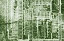
Figure
1. Photo of a Die Crack |
Damage
on the die
surface
can also cause die cracks. Improper equipment set-up can cause probe
needles, die overcoat dispense tools, etc. to land on the die and
fracture it. Excessive wirebonding force and energy can also cause cratering, or silicon fracture under the bond pad.
Excessive
mechanical stresses
on the package can also be transmitted down to the die, causing it to
crack. Even in relatively thick packages
like SOICs, these stresses may be transmitted down to the die without
damaging the package itself, making the problem even less detectable.
The common sources of these mechanical stresses are the
mechanical deflash, trim, and form processes, especially if the package
nests employed by the steps contain debris or particles that can act as
fulcrums for aggravating the stresses.
Die Cracking
may be
accelerated by SHRT,
Temp Cycle, and Thermal Shock.
See also:
Package
Failure Mechanisms;
Die Crack FA
Flow;
Die Attach; Failure Analysis
HOME
Copyright
©
2005.
EESemi.com.
All Rights Reserved.