Transistor-Transistor Logic (TTL)
Transistor-Transistor Logic,
or
TTL, refers to
the technology for designing and fabricating digital integrated
circuits that employ logic gates consisting primarily of bipolar transistors.
It overcomes the main problem associated with DTL, i.e., lack of speed.
The input to a TTL circuit is always through the emitter(s) of the input
transistor,
which exhibits a low input resistance.
The
base of the input transistor, on the other hand, is connected to the Vcc
line, which causes the input transistor to pass a current of about 1.6
mA when the input voltage to the emitter(s) is logic '0', i.e., near
ground. Letting a TTL input 'float' (left unconnected) will usually make
it go to logic '1', but such a state is vulnerable to stray signals,
which is why it is good practice to connect TTL inputs to Vcc using 1
kohm pull-up resistors.
The most
basic TTL circuit has a single output transistor configured as an
inverter with its emitter grounded and its collector tied to Vcc with a
pull-up resistor, and with the output taken from its
collector. Most
TTL circuits, however, use a
totem
pole output circuit, which
replaces the pull-up resistor with a Vcc-side transistor sitting on top of the GND-side
output transistor. The emitter of the Vcc-side transistor (whose collector is
tied to Vcc) is connected to the collector of the GND-side transistor
(whose emitter is grounded) by a diode. The output is taken from
the collector of the GND-side transistor.
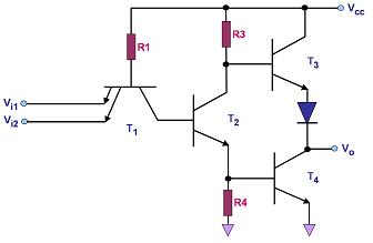
Figure 1 shows a basic 2-input TTL NAND gate with a totem-pole output.
 |
|
Figure 1.
A 2-input TTL NAND Gate with a Totem Pole Output Stage |
In the
TTL NAND gate of Figure 1, applying a logic '1' input voltage to
both
emitter inputs of T1 reverse-biases both base-emitter junctions, causing
current to flow through R1 into the base of T2, which is driven into
saturation. When T2 starts conducting, the stored base charge of T3
dissipates through the T2 collector, driving T3 into cut-off. On
the other hand, current flows into the base of T4, causing it to
saturate and pull down the output voltage Vo to logic '0', or near
ground. Also, since T3 is in cut-off, no current will flow from Vcc to the output, keeping it at logic '0'. Note that T2 always
provides complementary inputs to the bases of T3 and T4, such that T3
and T4 always operate in opposite regions, except during momentary
transition between regions.
On the
other hand, applying a logic '0' input voltage to
at least one
emitter
input of T1 will forward-bias the corresponding base-emitter junction,
causing current to flow out of that emitter. This causes the
stored base charge of T2 to discharge through T1, driving T2
into-cut-off. Now that T2 is in cut-off, current from Vcc will be
diverted to the base of T3 through R3, causing T3 to saturate. On
the other hand, the base of T4 will be deprived of current, causing T to
go into cut-off. With T4 in cut-off and T3 in saturation, the
output Vo is pulled up to logic '1', or closer to Vcc.
Outputs
of different TTL gates that employ the totem-pole configuration must
not
be connected together since differences in their output logic will cause
large currents to flow from the logic '1' output to the logic '0'
output, destroying both output stages.
The output of a typical TTL
gate under normal operation can sink currents of up to 16 mA.
The
noise margin
of a logic gate for logic level '0',
Δ0, is
defined as the difference between the maximum input voltage that it will
recognize as a '0' (Vil) and the maximum voltage that may be applied to
it as a '0' (Vol of the gate driving it). For logic level '1',
the
noise margin
Δ1
is
the
difference between the minimum input voltage that may be applied to it
as a '1' (Voh of the gate driving it) and the minimum input voltage that
it will recognize as a '1' (Vih). Mathematically,
Δ0 = Vil-Vol
and
Δ1 = Voh-Vih.
Any
noise that causes a noise margin to be overcome will result in a '0'
being erroneously read as a '1' or vice versa. In other words, noise
margin is a measure of the immunity of a gate from reading an input
logic level incorrectly. For TTL, Vil = 0.8V and Vol = 0.4V, so
Δ0 = 0.4V,
and Voh =
2.4V and Vih = 2.0 V, so
Δ1 = 0.4V.
These noise
margins are not as good as the noise margins exhibited by DTL.
As
mentioned earlier, TTL has a
much higher speed
than
DTL.
This is due to the fact that when the output transistor (T4 in Figure 1) is turned
off, there is a path for the stored charge in its base to dissipate
through, allowing it to reach cut-off faster than a DTL output
transistor. At the same time, the equivalent capacitance of the
output is charged from Vcc through T3 and the output diode, allowing the
output voltage to rise more quickly to logic '1' than in a DTL output
wherein the output capacitance is charged through a resistor.
The commercial names of
digital IC's that employ TTL start with '74', e.g., 7400, 74244, etc.
Most TTL devices nowadays, however, are named '74LSXXX', with the 'LS'
standing for 'low power Schottky'.
Low power schottky TTL
devices employ a
Schottly diode,
which is used to limit the voltage between the collector and the base of
a transistor, making it possible to design TTL gates that use
significantly less power to operate while allowing higher switching
speeds. See
also:
CMOS circuits.
See Also:
TTL Parameters; Logic
Gates; RTL; DTL; CMOS
HOME
Copyright
©
2005
www.EESemi.com.
All Rights Reserved.

