Semiconductor Photo Gallery
Cratering
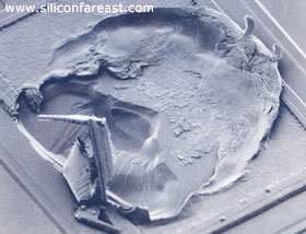
Figure 1.
Cratering - Silicon Damage Under the Bond Pad
Figure
1 shows a SEM photo of cratering, or the failure mechanism wherein the
silicon under the bond pad has been mechanically damaged. Gross
cases of cratering results in a chunk of the underlying silicon being
chipped off and dislodged from its place, forming a 'hole' or 'crater'
on the silicon substrate (hence the term 'cratering').
Cratering can
be due to several causes, but the most common reason for cratering is
over-bonding, or the situation wherein the bonding tool has transmitted
excessive stresses to the bond pad during wirebonding.
Cratering can result in lifted bonds, so an engineer analyzing a bond
lifting issue must look at the bond pad closely during investigation to
ensure that the appropriate corrective action will be taken.
See Also:
Wirebonding;
Bonding Failures
Back to
Semiconductor Photo Gallery
HOME